At the end of the last century, semiconductor lighting began to appear and develop rapidly. One of the core preconditions is the growth of blue GaN-based luminescent materials and the fabrication of device structures. The level of future materials and device structure technology will ultimately determine the height of semiconductor lighting technology. This chapter will focus on GaN-based materials and devices derived from equipment, source materials, device design, chip technology, chip applications and other links to analyze. In the current situation where large GaN single crystal materials cannot be prepared, MOCVD or metal organic chemical vapor deposition equipment is still the most critical device for heteroepitaxial growth of GaN materials. At present, the commercial MOCVD equipment market is mainly controlled by two international giants. In this situation, China's MOCVD has achieved great development, and there are 48 machines. But we still need to recognize the shortcomings of domestic MOCVD. For MOCVD, in general, the focus of research equipment is temperature control, and commercial equipment is uniformity, repeatability, and the like. At low temperatures, high In composition InGaN can be grown, suitable for long-wavelength applications of nitride system materials such as orange, red, and infrared, so that nitride applications can cover the entire white light field; and at 1200oC-1500oC, it can grow. The high Al composition of AlGaN allows the application of nitrides to expand into the field of ultraviolet and power electronics, with a wider range of applications. At present, foreign countries have 1600oC high temperature MOCVD equipment, which can produce high performance ultraviolet LED and power devices. China's MOCVD still needs long-term development, expanding the temperature control range of MOCVD; for commercial equipment, not only to improve performance, but also to ensure uniformity and scale. The source material source material mainly includes various gas materials, metal organic materials, substrate materials and the like. Among them, the substrate material is the weight of the weight, directly limiting the quality of the epitaxial film. At present, substrates of GaN-based LEDs are becoming more and more diversified, and substrate technologies such as SiC, Si, and GaN are gradually improved, and some substrates are developed from 2 inches to 3 inches, 4 inches, or even 6 inches, 8 inches, and the like. However, in general, the current price/performance ratio is still sapphire; SiC has superior performance but is expensive; the price and size advantage of Si substrate and the temptation to interface with traditional integrated circuit technology make Si substrate still the most promising technical route at the moment. one. GaN substrates still need to work hard to increase the size and lower the price, so that in the future, high-end green lasers and non-polar LED applications will play a significant role; metal organic materials from the dependence on imports to independent production, great progress; other gases Materials have also made great progress. In short, China has made great progress in the field of source materials. Epitaxial extension, the acquisition process of the device structure, is the most technologically advanced process step that directly determines the internal quantum efficiency of the LED. At present, most of the semiconductor lighting chips adopt multi-quantum well structure, and the specific technical route is often subject to the substrate material. The sapphire substrate generally adopts the pattern substrate (PSS) technology to reduce the density of the epitaxial film and improve the internal quantum efficiency, and also improve the light extraction efficiency. Future PSS technology is still an important substrate technology, and the size of graphics is gradually developing toward nanotechnology. The use of GaN homogeneous substrate can adopt non-polar surface or semi-polar surface epitaxial growth technology, partially eliminating the quantum Stark effect caused by polarized electric field, and has the application of green, yellow-green, red-orange GaN-based LED. Very important meaning. In addition, the current epitaxy generally prepares a single-emission wavelength quantum well. With appropriate epitaxial technology, it is possible to prepare a multi-wavelength emitting LED, that is, a single-chip white LED, which is also one of the promising technical routes. Among them, representative of the phase separation in the InGaN quantum well, the high In composition InGaN yellow light quantum dot and the blue quantum well combination are combined to emit white light. In addition, a multi-spectral illumination mode is realized by using multiple quantum well illumination to achieve a single-chip white light output, but the white light has a low color rendering index. Non-phosphorescent single-chip white LEDs are an attractive development direction. If high efficiency and high color rendering index can be achieved, the technology chain of semiconductor lighting will be changed. In terms of quantum well structure, the introduction of an electron blocking layer to block electron leakage and improve luminous efficiency has become a conventional method of LED epitaxial structure. In addition, optimizing the barrier and potential well of the quantum well will still be an important process. How to adjust the stress and realize band cutting can prepare LEDs with different emission wavelengths. How to improve the material quality of the p-type layer in terms of chip overlay? The p-type layer hole concentration, conductivity and the solution to the droop effect at high currents are still a top priority. In terms of chip technology, how to improve light extraction efficiency and obtain better heat dissipation scheme has become the main purpose of chip design, and correspondingly developed vertical structure, surface roughening, photonic crystal, flip-chip structure, film flip-chip structure (TFFC), New transparent electrodes and other technologies. Among them, the film flip-chip structure uses laser stripping, surface roughening and other techniques to greatly improve the light extraction efficiency. The chip application has low fluorescence conversion efficiency for white LED technology solutions for blue LEDs to excite yellow phosphors. RGB multi-chip white light and single-chip non-phosphor white light have become the main technical trends of future white LEDs, and the less efficient green LEDs have become The main limiting factor of RGB multi-chip white light, future semi-polar or non-polar green LED will become an important development trend. In solving the white LED color development, the RGB three-color phosphor can be excited by the violet or ultraviolet LED to obtain the high color rendering white LED technology, but a part of the efficiency is inevitably sacrificed. At present, the efficiency of violet or ultraviolet chip has been greatly improved. The external quantum efficiency of 365nm wavelength UV LED produced by Nichia Chemical Co., Ltd. is close to 50. In the future, UV LED will gain more applications and no other UV luminescent system materials will be replaced. The outlook is huge. Some developed countries have invested a lot of manpower and material resources to carry out research on UVLED. The application of the red-light infrared band of nitrides, in addition to the environment, is difficult to compete with arsenic in terms of price and performance, so the prospects are not very clear. According to the above explanation, the upstream materials and equipment surrounding semiconductor illumination have been greatly developed. Especially in terms of efficiency, the blue light band is close to the ideal efficiency, and the price ratio of the chip in the semiconductor lighting fixture is also greatly reduced. The efficiency of light develops towards light quality, which requires chip materials to break through the blue light field and develop toward long wavelengths and short wavelengths, while green, violet and ultraviolet LED chips will be the focus of research.
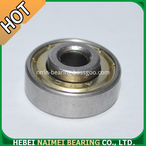
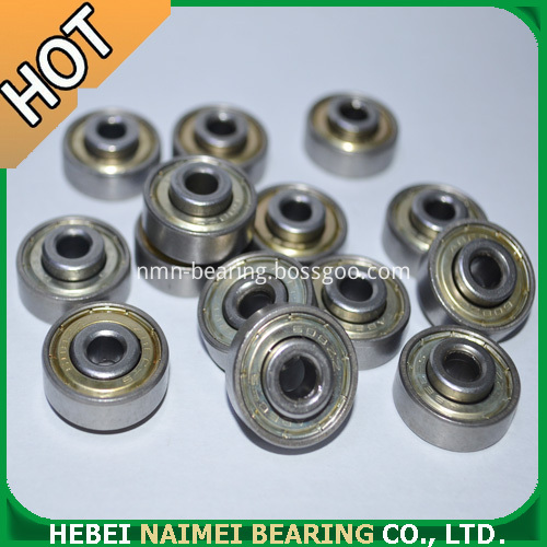
Higher Inner Ring Ball Bearing : Hebei Naimei Bearing Co., Ltd. is specilized in Higher Inner Ring Ball bearings . it is one of Non-srtandard bearings . We have completed processed system. the several Auto- professional machines to guarantee the Quality. Our products are sold to America,Europe Oceania etc. We are the trustworthy team who works for the customers.
- Bearing Model: Miniature Bearing 626 608;
-
Characteristics: Inner Ring Higher on One Side or Two Sides;
- Bearing Inner Ring Width: In Accordance With Customers' Design, Sample or Drawing


If you need other styles Non-standard bearings , please send us your drawing or samples , we have professional technical department service to you .
Higher Inner Ring Ball Bearing
Higher Inner Ring Ball Bearing,Ring Ball Bearing,Window Sliding Bearing,Plastic Injected Roller Bearing
Hebei Naimei Bearing Co., Ltd. , http://www.nmn-bearing.com
![<?echo $_SERVER['SERVER_NAME'];?>](/template/twentyseventeen/skin/images/header.jpg)